
Confidential Semiconductor Manufacturer LFAB2
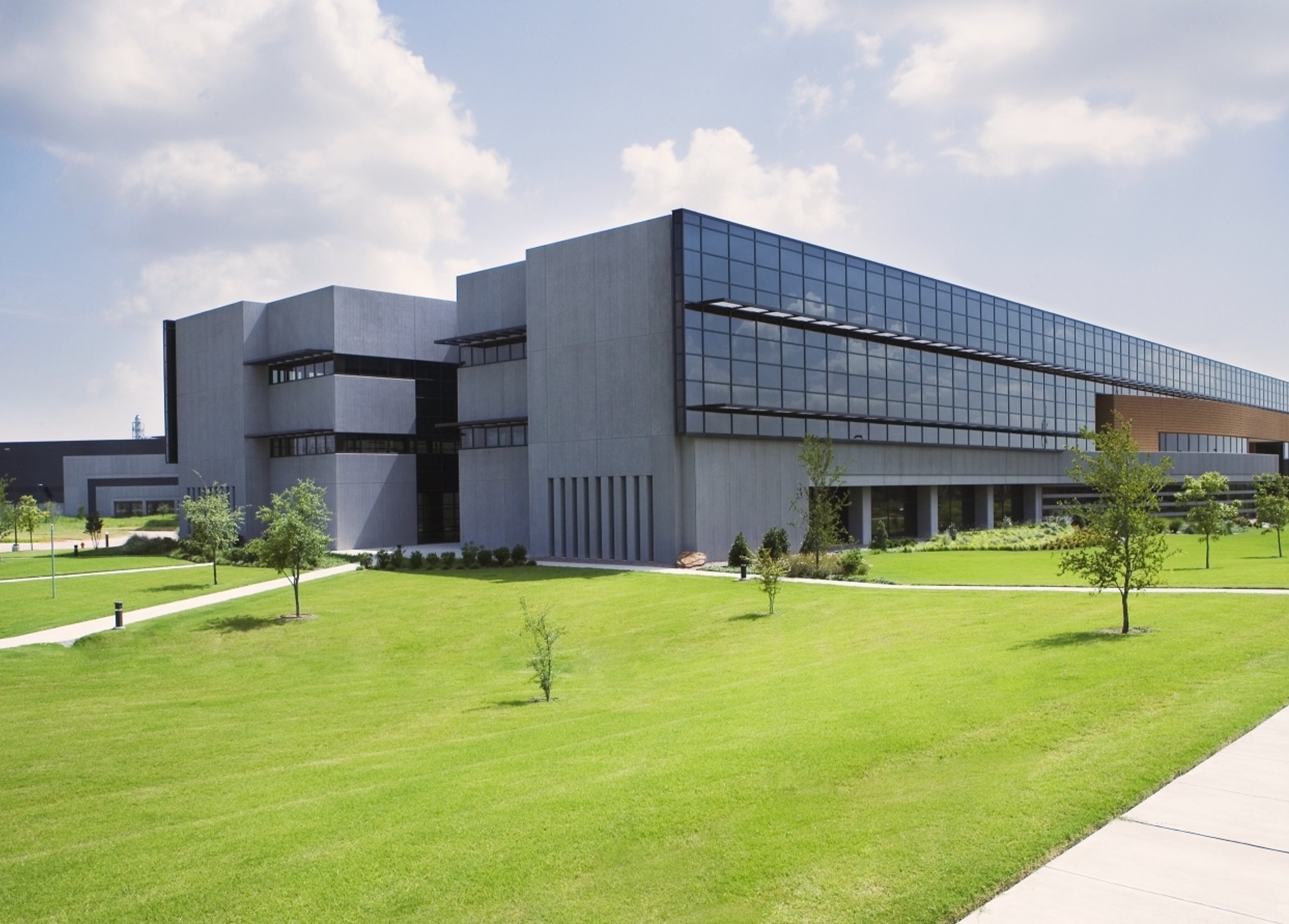
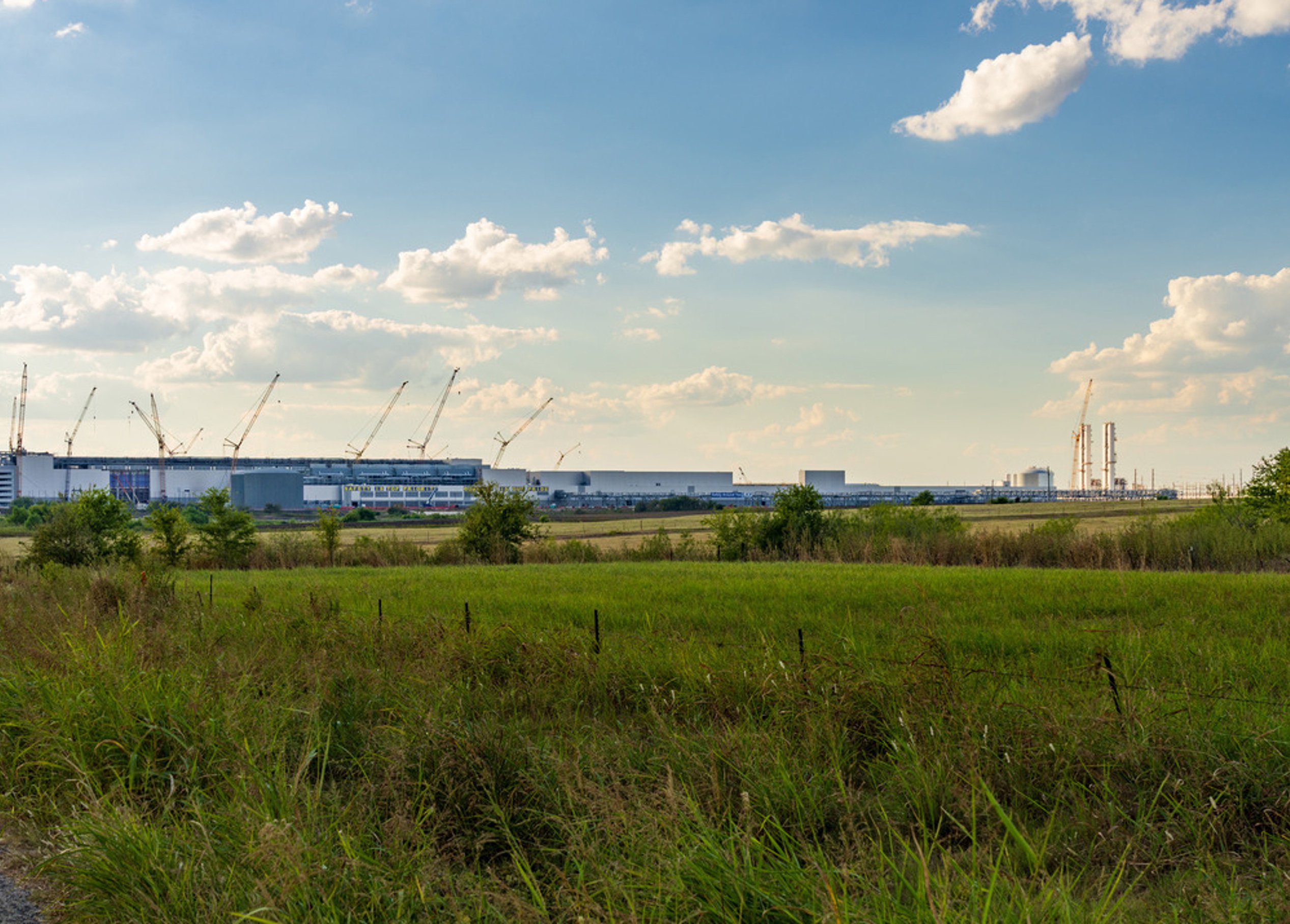
This 2.2-million-square-foot semiconductor wafer Fab is engineered for unmatched precision, efficiency, and sustainability, setting a new standard for advanced manufacturing. At its core, a 380,000-square-foot cleanroom anchors the facility, supported by two levels of sub-fab infrastructure designed for seamless operation and adaptability.
The Fab integrates essential cleanroom support functions, including wafer start and finishing, parametric testing, personnel gowning facilities, and chemical storage and distribution, alongside dedicated bulk chemical storage and a standalone central utility plant. A robust wastewater treatment system and an independent power source ensure reliability and resilience in an increasingly complex supply chain.
Designed to push the boundaries of sustainable innovation, the facility is targeting LEED Gold certification from the U.S. Green Building Council, reinforcing its commitment to environmental stewardship while delivering the infrastructure needed to drive the future of semiconductor technology.
Similar projects
/

Talk with us
Complex challenges need fresh perspectives and deep expertise. Connect with our team to explore how we can help you create spaces that make a real difference.