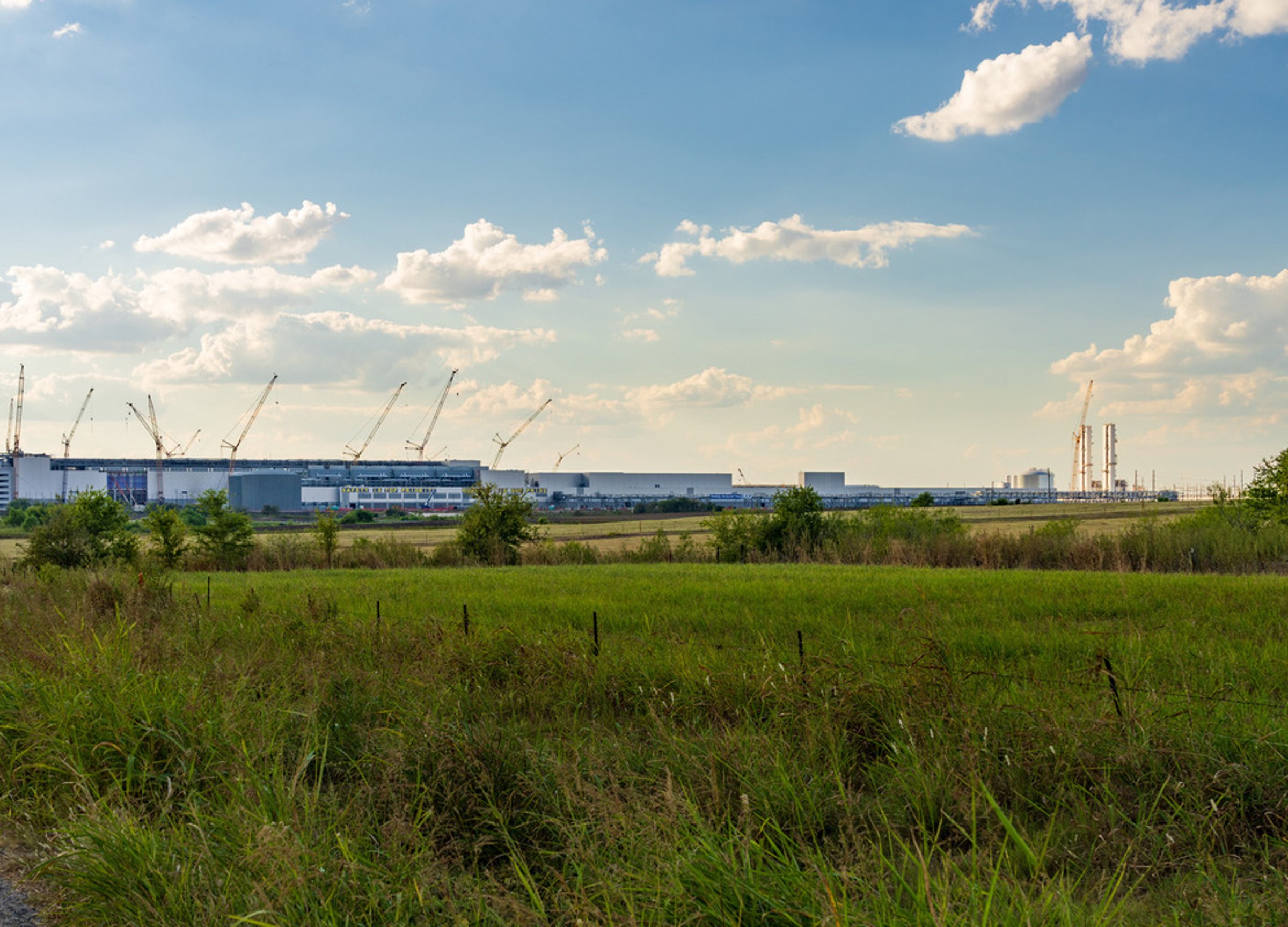
Confidential Semiconductor Manufacturer T-Projects
The T1-PH1 Fit-Up project represents a groundbreaking advancement in semiconductor manufacturing. Designed to support the next generation of technological innovation, this 4,811,500-square-foot facility features a comprehensive approach to gas and chemical systems, cleanroom environments, bulk specialty gas facilities, and essential warehouse infrastructure. Page played a pivotal role in engineering and design, ensuring seamless integration and high-performance solutions.
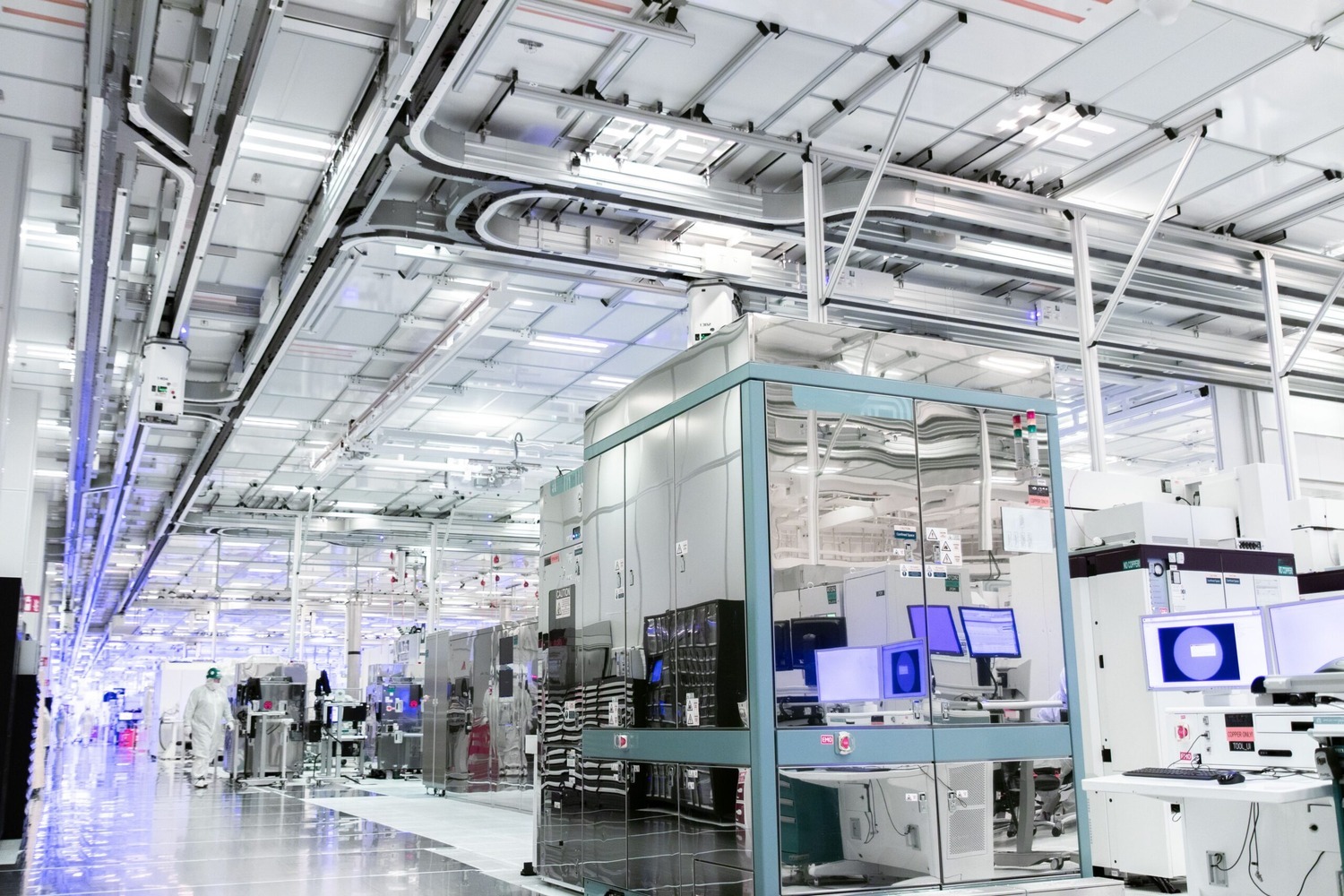
Gas, Chemical & Slurry (GCS) Systems
As part of the Gas, Chemical & Slurry (GCS) Systems scope, Page developed storage and distribution systems for a new greenfield fabrication facility. This involved the precise design of specialty gas and process chemical handling, including waste chemical management. Page provided extensive technical services such as chemical classification, equipment layout, utility hookup design, system sizing calculations, and advanced modeling for piping flow and stress analysis. These elements were critical in securing necessary permits and ensuring smooth construction execution.
Cleanroom
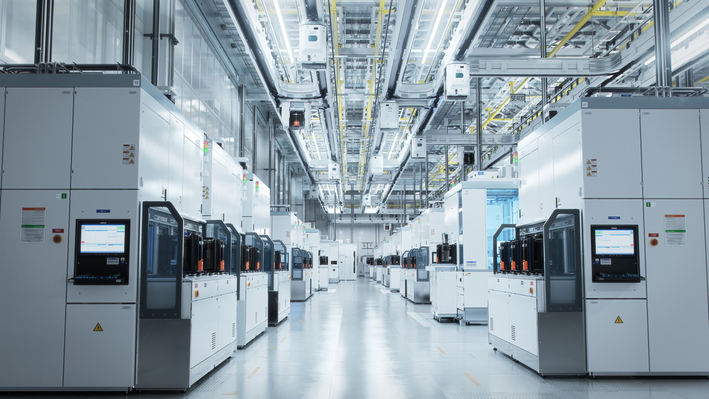
FAB1 boasts 1.2 million square feet of class-1 cleanrooms, including Fabrication and Sub FAB areas. As engineer of record, Page led architecture, structural, mechanical, process, electrical, and Instrumentation & Controls (I&C) engineering. We provided engineering analysis, managed permitting, attended client meetings, and oversaw construction. The cleanroom package included 3,000+ construction drawings.
Bulk Specialty Gas (BSGS) & ISO Yard
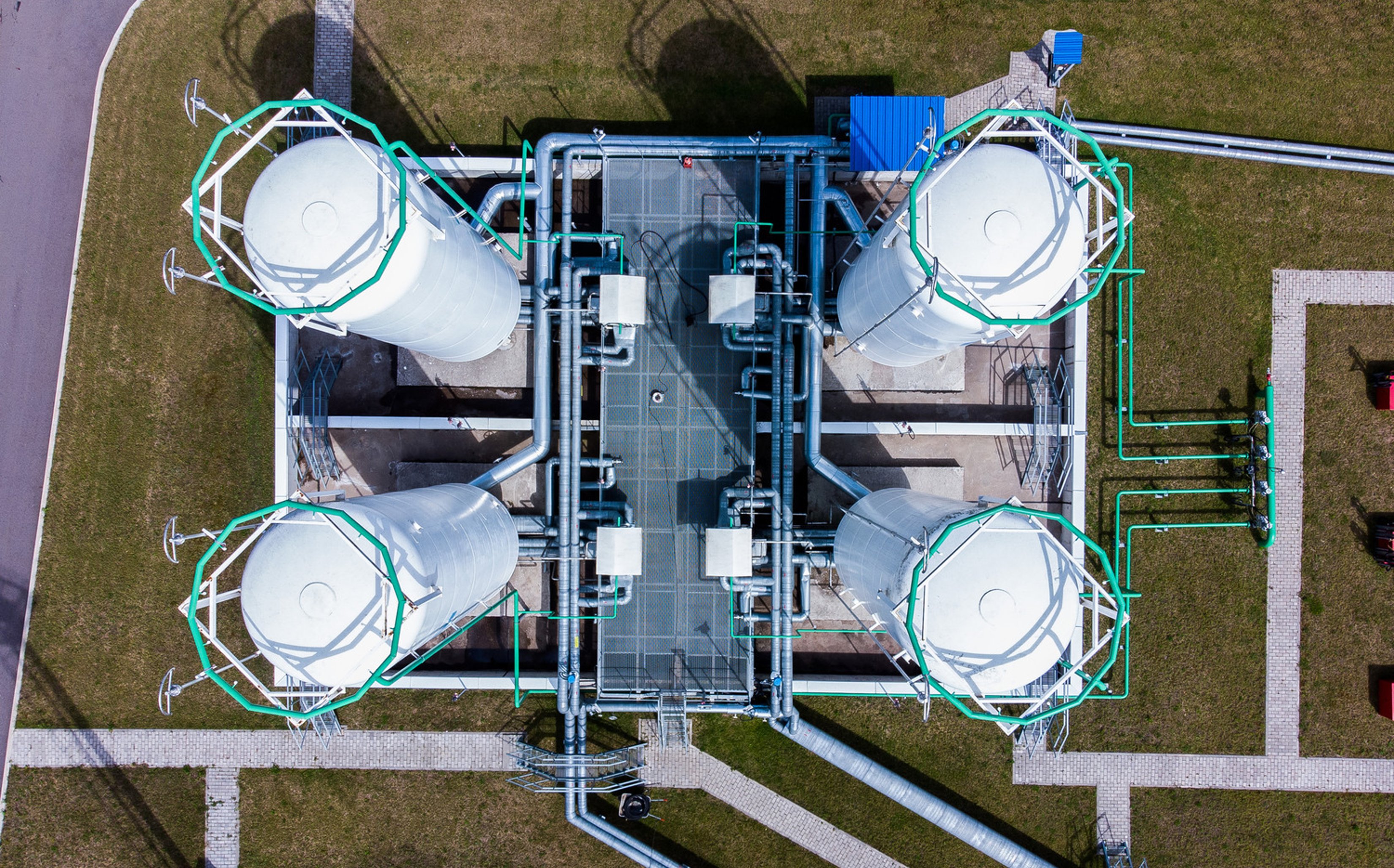
The Bulk Specialty Gas (BSGS) & ISO Yard was developed as a turn-key project within a broader campus initiative to support semiconductor production. This facility enables the manufacturing of advanced logic chips used in high-performance computing, 5G, and artificial intelligence applications.
Key features include:
- Integrated Control Buildings: three dedicated buildings for real-time monitoring and management.
- Specialized ISO Canopies: six canopies designed for safe handling of H2/N2, SiH4, NH3, He, N2O, and NF3 gases.
- Dedicated HCl and CO2 Facilities: HCl ISO building and CO2 tank with supporting equipment pad.
- Grade-Supported Equipment Pads: stable foundation ensuring safety and operational integrity.
- Multi-Level Utility Bridge: Optimizing connectivity across facility infrastructure.
Warehouses
Beyond the fabrication infrastructure, Page led the development of warehouse facilities, comprising eight buildings with a total footprint of 280,000 square feet. These warehouses serve vital functions, including secure chemical storage, emergency response, hardware innovation, waste segregation, and hazardous waste management. The Hardware Innovation Center provides space for research and prototyping, while the Wafer Granulator supports production efficiency. To enhance overall site functionality, Page provided civil and landscape design, electrical and mechanical engineering, fire protection planning, and permitting services.
T1-PH2 core and shell
The T1-PH2 Core and Shell project introduces a new three-story semiconductor FAB building adjacent to the existing FAB1. This 2.71-million-square-foot structure required comprehensive architectural and structural engineering expertise. Page’s contributions included civil engineering for underground utilities encased in the concrete foundation, such as electrical, plumbing, telecom, and fire protection systems. Drawing from lessons learned in constructing the adjacent FAB, the team applied value engineering strategies to refine the design for efficiency, cost-effectiveness, and long-term sustainability.
Through each of these projects, Page played a pivotal role in bringing to life an advanced semiconductor manufacturing environment. Our expertise in multidisciplinary design, engineering, and construction oversight has ensured the seamless integration of high-performance solutions tailored to meet the evolving needs of the semiconductor industry.
Similar projects
/

Talk with us
Complex challenges need fresh perspectives and deep expertise. Connect with our team to explore how we can help you create spaces that make a real difference.